- 您现在的位置:买卖IC网 > Sheet目录335 > IXBD4410PI (IXYS)IC LOW SIDE DRIVER 16DIP
IXBD4410
IXBD4411
Symbol
Definition
Maximum Ratings
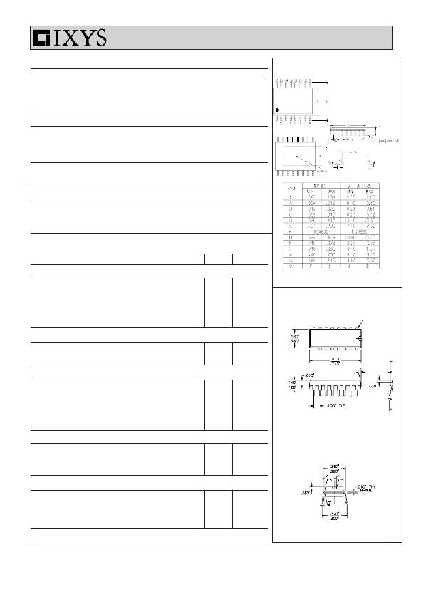
Dimensions in inch (1" = 25.4 mm)
V DD /V EE
V in
I in
I o (rev)
P D
P D
T A
T JM
T stg
T L
Supply Voltage
Input Voltage (INH, INL)
Input Current (INL, INH, IM)
Peak Reverse Output Current (OUT)
Maximum Power Dissipation (T A = 25 ° C)
T C = 25 ° C (16-Pin SOIC)
Operating Ambient Temperature
Maximum Junction Temperature
Storage Temperature Range
Lead Soldering Temperature for 10 s
-0.5 ... 24
-0.5...V DD +0.5
± 10
2
600
10
-40 ... 85
150
-55 ... 150
300
V
V
A
A
mW
W
° C
° C
° C
° C
16-Pin SOIC
R thJA
R thJC
(16-Pin SOIC)
1.67
10
K/W
K/W
Die substrate
connected to tab
Recommended Operating Conditions
V DD /V EE
V DD /LG
L Gh /L Gl
Supply Voltage
Maximum Common Mode dv/dt
10 ... 20 V
10 ... 16.5 V
± 50 V/ns
Symbol
Definition/Condition Characteristic Values
(T A = 25 ° C, V DD = 15 V, unless otherwise specified)
min. typ. max.
INL, INH Inputs (referred to LG)
V t+
V t-
Positive-Going Threshold
Negative-Going Threshold
3.65
1
V
V
V ih
I in
Input Hysteresis
Input Leakage Current/V in =V DD or LG
-1
1
1
V
μ A
16-Pin Plastic DIP
C in
Input Capacitance
10
pF
Open Drain Fault Output (referred to LG)
V oh
HI Output/R pu = 10 k ? to V DD
V DD -0.05
V
V ol
LO Output/I o = 4 mA
0.3
0.5
V
OUT Output (referred to LG)
V oh
HI Output/I o = -5 mA
V DD -0.05
V
V ol
R o
R o
LO Output/I o = 5 mA
Output HI Res./I o = -0.1 A
Output LO Res./I o = 0.1 A
V EE +0.05
3
3
5
4
V
?
?
I pk
Peak Output Current/C L = 10 nF
1.5
2
A
IM Input (referred to KG)
End view
V t+
C in
R s
Positive-Going Threshold
Input Capacitance
Shorting Device Output Resistance
0.24
50
0.3
10
75
0.45
100
V
pF
?
VEE Supply (referred to LG)
V EE
I out
f inv
V EEF
Output Voltage/I o = 1 mA, C o = 1 μ F
Output Current/V out = 0.70 ? V EE
Inverting Frequency
Undervoltage Fault Indication
-5
-20
-3
-6.5
-25
600
-7.5
-4.8
V
mA
kHz
V
? 2004 IXYS All rights reserved
发布紧急采购,3分钟左右您将得到回复。
相关PDF资料
IXD611S7T/R
IC DRVR HALF BRIDGE 600MA 14SOIC
IXDD404SIA-16
IC MOSFET DRVR DUAL 4A 16-SOIC
IXDD408YI
IC MOSFET DRVR LS 8A SGL 5TO-263
IXDD414SI
IC MOSFET DRVR 14A LOSIDE 14SOIC
IXDD509D1T/R
IC GATE DRIVER 9A 6-DFN
IXDD614CI
MOSFET N-CH 14A LO SIDE TO-220-5
IXDE504SIAT/R
IC GATE DRIVER 4A 8-SOIC
IXDE514SIAT/R
IC GATE DRIVER 14A 8-SOIC
相关代理商/技术参数
IXBD4410SI
功能描述:功率驱动器IC 1/2Bridge2A RoHS:否 制造商:Micrel 产品:MOSFET Gate Drivers 类型:Low Cost High or Low Side MOSFET Driver 上升时间: 下降时间: 电源电压-最大:30 V 电源电压-最小:2.75 V 电源电流: 最大功率耗散: 最大工作温度:+ 85 C 安装风格:SMD/SMT 封装 / 箱体:SOIC-8 封装:Tube
IXBD4411
制造商:IXYS 制造商全称:IXYS Corporation 功能描述:ISOSMART Half Bridge Driver Chipset
IXBD4411PC
制造商:未知厂家 制造商全称:未知厂家 功能描述:Interface IC
IXBD4411PI
功能描述:功率驱动器IC 1/2Bridge2A RoHS:否 制造商:Micrel 产品:MOSFET Gate Drivers 类型:Low Cost High or Low Side MOSFET Driver 上升时间: 下降时间: 电源电压-最大:30 V 电源电压-最小:2.75 V 电源电流: 最大功率耗散: 最大工作温度:+ 85 C 安装风格:SMD/SMT 封装 / 箱体:SOIC-8 封装:Tube
IXBD4411SI
功能描述:功率驱动器IC 1/2Bridge2A RoHS:否 制造商:Micrel 产品:MOSFET Gate Drivers 类型:Low Cost High or Low Side MOSFET Driver 上升时间: 下降时间: 电源电压-最大:30 V 电源电压-最小:2.75 V 电源电流: 最大功率耗散: 最大工作温度:+ 85 C 安装风格:SMD/SMT 封装 / 箱体:SOIC-8 封装:Tube
IXBD4412PC
制造商:未知厂家 制造商全称:未知厂家 功能描述:Interface IC
IXBD4412PI
制造商:未知厂家 制造商全称:未知厂家 功能描述:Interface IC
IXBD4413PC
制造商:未知厂家 制造商全称:未知厂家 功能描述:Interface IC
